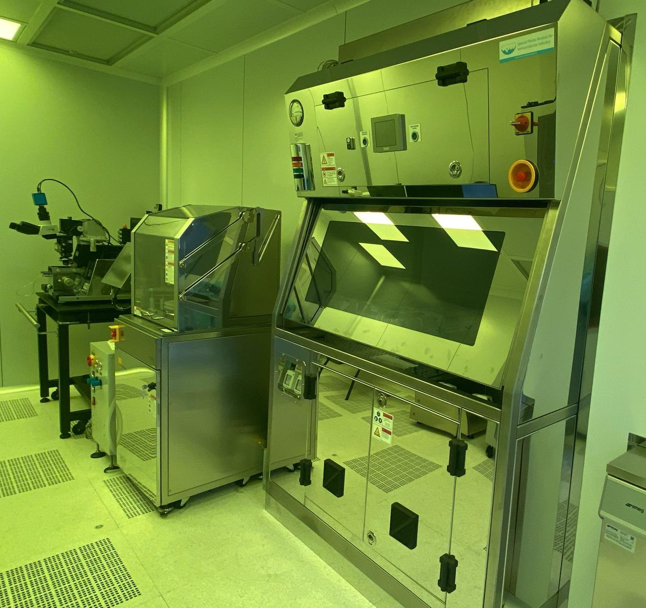
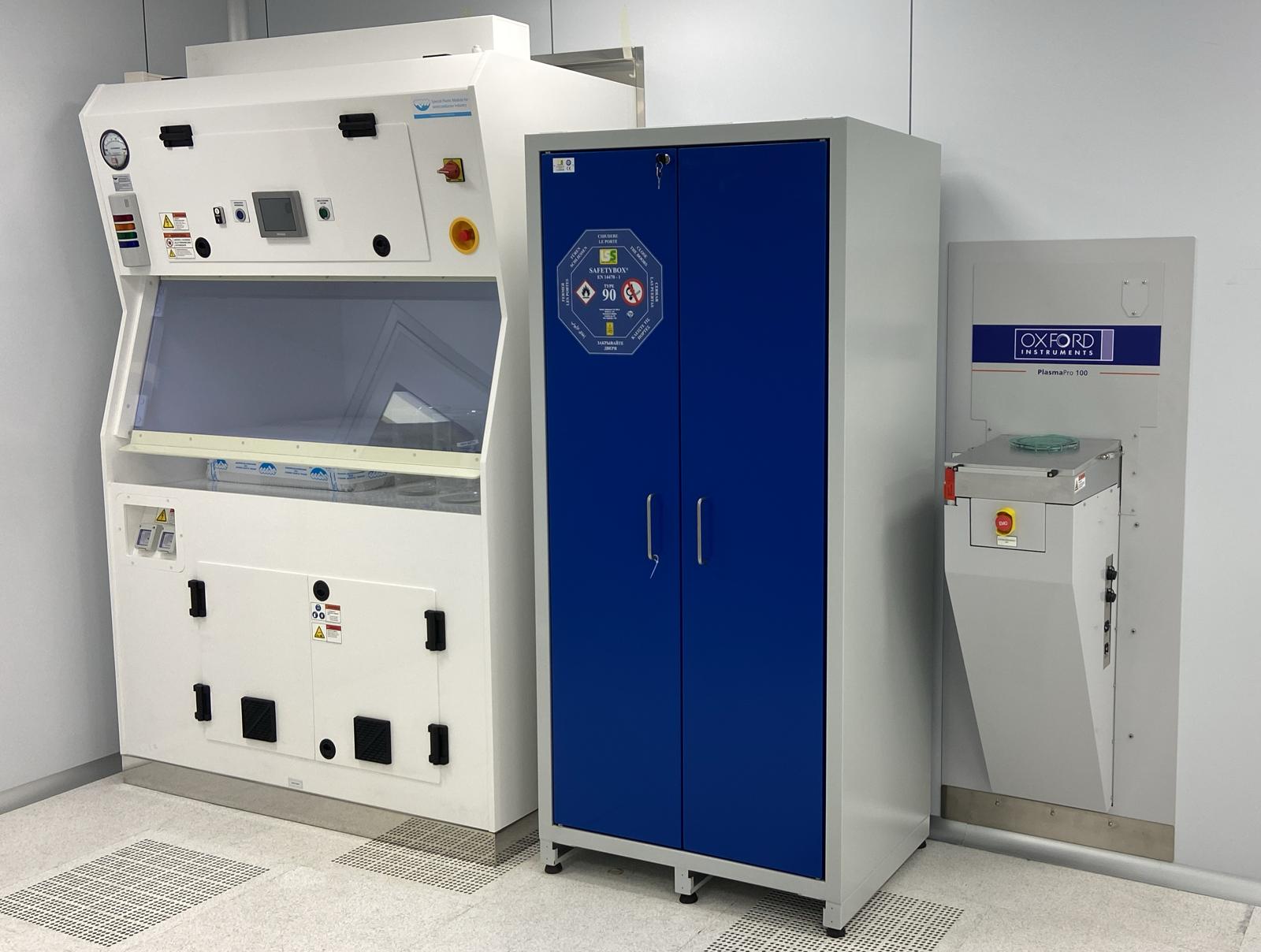
Cleanroom Our ISO-certified cleanroom facility provides researchers with access to state-of-the-art nanofabrication equipment in a controlled environment. The facility supports a wide range of research activities including semiconductor device fabrication, superconductors development, photonics, and materials science.
Nanoscale Lithography The nanofabrication area includes high-resolution patterning systems for device definition at the nanoscale. The JEOL 8100 Electron Beam Lithography system (100 kV) achieves resolutions down to 8 nm, supporting both high-resolution and high-throughput modes for complex nanostructures for applications in quantum devices, nanophotonics, and microelectronics. The Heidelberg 66WL Laser Writer enables rapid, maskless lithography with submicron precision on various substrates, while the Mask Aligner supports contact, proximity, and vacuum exposure modes for substrates up to 4 inches. Ideal for MEMS, microfluidics, and semiconductor prototyping, the MJB4 features manual operation with intuitive controls and flexible mask handling.
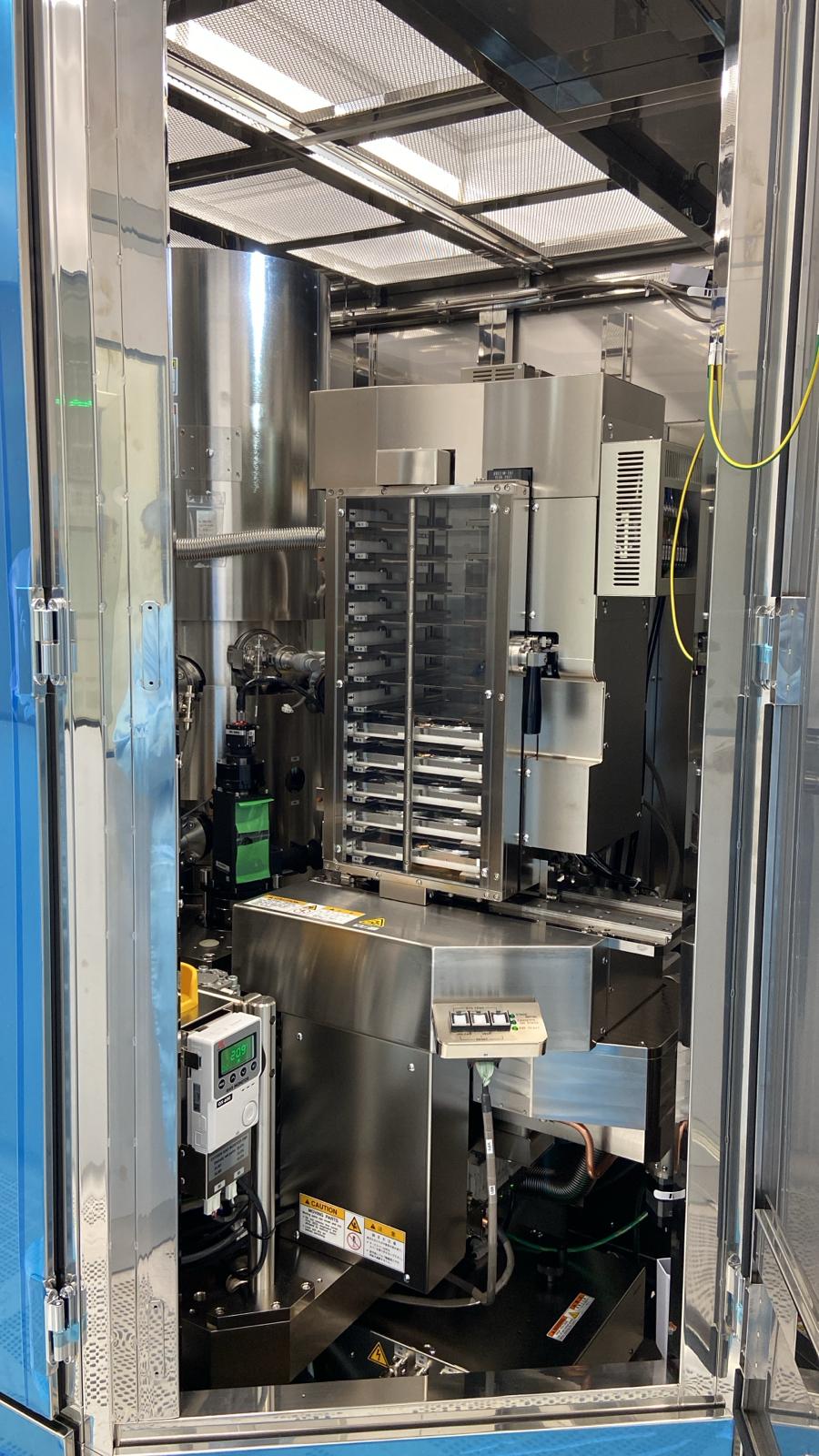
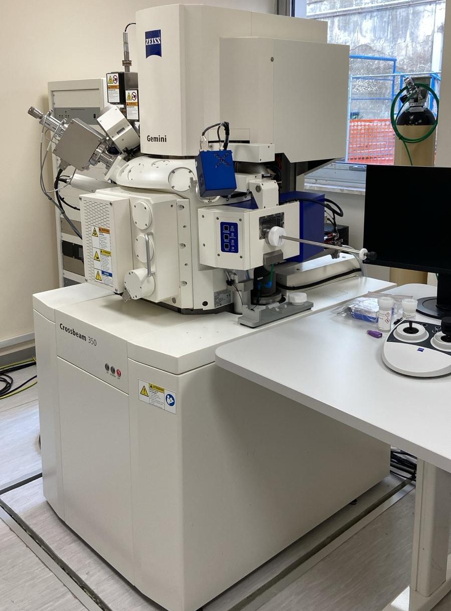
Physical and Chemical Etching Material pattern transfer and nanostructure definition are performed using a RIE Cobra plasma etcher, providing uniform and anisotropic etching across a wide range of materials. The Gemini FIB-SEM combines focused ion beam milling with high-resolution imaging, allowing precise cross-sectioning, 3D tomography, and correlative analysis of nanoscale devices.
Wet Benches and Nanoscale Characterization For structural and electrical analysis, the lab hosts a Gemini 2 FE-SEM for high-resolution imaging below 1 kV, a Park AFM for non-contact topography and property mapping, and a manual probe station for electrical testing of wafers up to 200 mm. Complementary wet benches are available for cleaning, chemical treatment, and sample development.